- Raspberry Pi & Accessories
- Raspberry Pi Kits
- Raspberry Pi Board
- Raspberry Pi Case
- Raspberry Pi Came
- Raspberry Pi Accessories

74LS And 74HC Series IC
Compare
T74LS05B1 T74LS 05B1 S05B1 AND Gate IC in Pakistan
T74LS05B1 T74LS 05B1 S05B1 AND Gate IC in Pakistan
₨98
T74LS05B1 T74LS 05B1 S05B1 AND Gate IC in Pakistan
Add a review
You must be logged in to post a review
Log In
Related products
- 74LS And 74HC Series IC
74LS189 64 Bit RAM with 3 State Output IC 74189 74HC189 in Pakistan
Quick View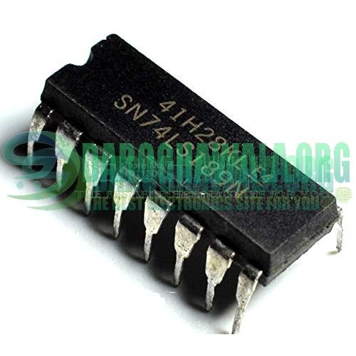 74LS And 74HC Series IC
74LS189 64 Bit RAM with 3 State Output IC 74189 74HC189 in Pakistan
The 74LS189 is a high-speed 64-bit RAM organized as a 16-word by the 4-bit array. Address inputs are buffered to minimize loading and are fully decoded on-chip. The outputs are 3-state and are in the high impedance state whenever the Chip Select (CS) input is HIGH. The outputs are active only in the read mode and the output data is the complement of the stored data.
SKU: D2011 - 74LS And 74HC Series IC
SMD 74HC595 74HC595D SOP16 Patch 8 Bit Serial Shift Register in Pakistan
Quick View 74LS And 74HC Series IC
SMD 74HC595 74HC595D SOP16 Patch 8 Bit Serial Shift Register in Pakistan
74HC595 8-bit Serial-to-Parallel Shift Register is a high-speed shift register that utilizes advanced silicon-gate CMOS technology. This device possesses the high noise immunity and low power consumption of standard CMOS integrated circuits, as well as the ability to drive 15 LS-TTL loads.
This device contains an 8-bit serial-in, parallel-out shift register that feeds an 8-bit D-type storage register. The storage register has 8 3-STATE outputs. Separate clocks are provided for both the shift register and the storage register.
The shift register has direct-overriding clear, serial input, and serial output (standard) pins for cascading. Both the shift register and storage register use positive-edge triggered clocks. If both clocks are connected together, the shift register state will always be one clock pulse ahead of the storage register.
The 74HC logic family is speed, function, and pin-out compatible with the standard 74LS logic family. All inputs are protected from damage due to static discharge by internal diode clamps to VCC and ground.
SKU: D2013 - 74LS And 74HC Series IC
74LS76 DUAL JK FLIP-FLOP IC in Pakistan
74LS76 comes with dual JK flip-flops. JK flip flops are widely used in daily electronics devices by many methods but the basic operation of the JK flip flop is to store a bit. JK flip flop allows it to store a bit and then allows it to use for further functions. in digital electronics circuits. JK flip flop is one of the popular flip flops due to its clock input, pre-set, and clear functionalities. The JK flip-flop changes its state under the clock pulse signal. The clock signal can be either a positive edge or a negative edge. The clock pulse gives multiple advantages to the flip-flop. 74LS76 also has provided a feature to neglect or prevent invalid outputs.
SKU: D2025 - 74LS And 74HC Series IC
74151 ic in Pakistan
This Data Selector/Multiplexer contains full on-chip decoding to select one-of-eight data sources as a result of a unique three-bit binary code at the Select inputs. Two complementary outputs provide both inverting and non-inverting buffer operation. A Strobe input is provided which, when at the high level, disables all data inputs and forces the Y output to the low state and the W output to the high state. The Select input buffers incorporate internal overlap features to ensure that select input changes do not cause invalid output transients. RoboticsBD
SKU: D2022


Reviews
There are no reviews yet