

NAND Gate CD4011 IC CMOS Quad 2 Input NAND Gate In Pakistan
CD4011BE IC CMOS Quad 2 Input NAND Gate is a logic gate that produces an output that is false only if all its inputs are true. CD4011BE IC CMOS Quad 2 Input NAND Gate are NAND gates that provide the system designer with direct implementation of the NAND function and supplement the existing family of CMOS gates. All inputs and outputs are buffered.
The CD4011B, CD4012B, and CD4023B types are supplied in 14-lead hermetic dual-in-line ceramic packages (F3A suffix), 14-lead dual-in-line plastic packages (E suffix), 14-lead small-outline packages (M, MT, M96, and NSR suffixes), and 14-lead thin shrink small-outline packages (PWR suffix). The CD4011B and CD4023B types also are supplied in 14-lead thin shrink small-outline packages (PW suffix).
₨85
CD4011BE IC CMOS Quad 2 Input NAND Gate is a logic gate that produces an output that is false only if all its inputs are true. CD4011BE IC CMOS Quad 2 Input NAND Gate are NAND gates that provide the system designer with direct implementation of the NAND function and supplement the existing family of CMOS gates. All inputs and outputs are buffered.
The CD4011B, CD4012B, and CD4023B types are supplied in 14-lead hermetic dual-in-line ceramic packages (F3A suffix), 14-lead dual-in-line plastic packages (E suffix), 14-lead small-outline packages (M, MT, M96, and NSR suffixes), and 14-lead thin shrink small-outline packages (PWR suffix). The CD4011B and CD4023B types also are supplied in 14-lead thin shrink small-outline packages (PW suffix).
Features of CD4011BE IC CMOS Quad 2 Input NAND Gate:
- Propagation delay time = 60 ns (typ.) at CL = 50 pF, VDD = 10 V
- Buffered inputs and outputs
- Standardized symmetrical output characteristics
- The maximum input current of 1 µA at 18 V over-full package temperature range; 100 nA at 18 V and 25°C
- 100% tested for quiescent current at 20 V
- 5-V, 10-V, and 15-V parametric ratings
- Noise margin (over full package temperature range:
1 V at VDD = 5 V
2 V at VDD = 10 V
2.5 at VDD = 15 V - Meets all requirements of JEDEC Tentative Standard No. 13B, “Standard Specifications for Description of “B” Series CMOS Devices”
Specifications of CD4011BE IC CMOS Quad 2 Input NAND Gate:
| Description | Value |
| Lead Finish | Gold |
| Logic Function | NAND |
| Maximum Operating Supply Voltage | 18 V |
| Maximum Propagation Delay Time @ Maximum CL | 250@5V|120@10V|90@15V ns |
| Maximum Quiescent Current | 5 uA |
| Minimum Operating Supply Voltage | 3 V |
| Mounting | Through Hole |
| Operating Temperature | -55 to 125 °C |
| Pin Count | 14 |
| Product Dimensions | 19.05 x 6.35 x 3.3 mm |
| Supplier Package | PDIP |
| Typical Quiescent Current | 0.02 uA |
Package Include:
- 1x CD4011BE NAND Gate
Related products
- Power Management ICs
ULN2803 ULN2803A ULN2803APG IC In Pakistan
The ULN2803A is a high-voltage, high-current Darlington transistor array. The device consists of eight NPN Darlington pairs that feature high-voltage outputs with common-cathode clamp diodes for switching inductive loads. The collector-current rating of each Darlington pair is 500 mA. The Darlington pairs may be connected in parallel for higher current capability. Applications include relay drivers, hammer drivers, lamp drivers, display drivers (LED and gas discharge), line drivers, and logic buffers. The ULN2803A has a 2.7-k series base resistor for each Darlington pair for operation directly with TTL or 5-V CMOS devices
SKU: D2083 - Power Management ICs
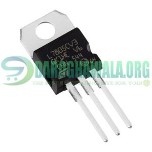
LM7805 L7805 7805 Linear Voltage Regulator IC In Pakistan
The LM7805CV is a fixed output, three-terminal precision positive voltage regulator in 3 pins TO-220 package. This regulator can provide local on-card regulation by eliminating distribution problems associated with single-point regulation. The L7805 fixed voltage regulator is designed with thermal overload protection that shuts down the circuit when subjected to an excessive power overload condition, internal short circuit protection that limits the maximum current the circuit will pass, and output transistor safe area compensation that reduces the output short circuit as the voltage across the pass transistor is increased. If adequate heat sinking is provided then this positive voltage regulator can deliver over 1A output current.
SKU: D1190 - Power Management ICs
LM7812 L7812 7812 Linear Voltage Regulator IC In Pakistan
The LM7812CV is a three-terminal positive Voltage Regulator with several fixed output voltages, making it useful in a wide range of applications. This regulator can provide local on-card regulation, eliminating the distribution problems associated with single-point regulation. Each type employs internal current limiting, thermal shutdown, and safe area protection, resulting in it being essentially indestructible. If adequate heat sinking is provided, they can deliver over 1A output current. Although designed primarily as fixed voltage regulators, these devices can be used with external components to obtain adjustable voltage and currents.
SKU: D1192 - Power Management ICs
DIP-8 gate drivers ic chip IR2104 in Pakistan
Fully operational to +600V Tolerant to negative transient voltage dV/dt immune Gate drive supply range from to 20V Undervoltage lockout 3.3V, 5V and 15V input logic compatible Cross-conduction prevention logic Internally set deadtime High side output in phase with input Shut down input turns off both channels Matched propagation delay for both channels
SKU: D2085 - Power Management ICs
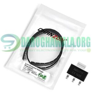
AMS1117 3.3V 1A SMD SOT-223 DC Voltage Regulator IC In Pakistan
The AMS1117 series of adjustable and fixed voltage regulators are designed to provide up to1A output current and to operate down to 1V input-to-output differential. The dropout voltage of the device is guaranteed a maximum of 1.3V, decreasing at lower load currents.
On-chip trimming adjusts the reference voltage to 1.5%. The current limit is set to minimize the stress under overload conditions on both the regulator and power source circuitry. The AMS1117 devices are pin-compatible with other three-terminal SCSI regulators and are offered in the low profile surface mount SOT-223 package, in the 8L SOIC package, and in the TO-252 (DPAK) plastic package.SKU: D300


Reviews
There are no reviews yet