- Raspberry Pi & Accessories
- Raspberry Pi Kits
- Raspberry Pi Board
- Raspberry Pi Case
- Raspberry Pi Came
- Raspberry Pi Accessories


74LS And 74HC Series IC
Compare
7428 Quad Two input NOR in Pakistan
7428 Quad Two input NOR in Pakistan
₨99
7428 Quad Two input NOR in Pakistan
Packing list:
- 1x 7428 Quad Two input NOR
Add a review
You must be logged in to post a review
Log In
Related products
- 74LS And 74HC Series IC
7447 74HC47 74LS47 BCD to 7 Segment Decoder Driver DIP 16 in Pakistan
Quick View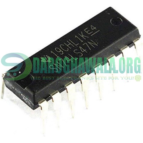 74LS And 74HC Series IC
7447 74HC47 74LS47 BCD to 7 Segment Decoder Driver DIP 16 in Pakistan
74LS47 accepts four lines of BCD (8421) input data, generates their complements internally and decodes the data with seven AND/OR gates having open-collector outputs to drive indicator segments directly. Each segment output is guaranteed to sink 24 mA in the ON (LOW) state and withstand 15V in the OFF (HIGH) state with a maximum leakage current of 250 µA. Auxiliary inputs provided blanking, 74LS47 BCD to 7-Segment Decoder/Driver IC.
SKU: D2008 - 74LS And 74HC Series IC
SMD 74HC595 74HC595D SOP16 Patch 8 Bit Serial Shift Register in Pakistan
Quick View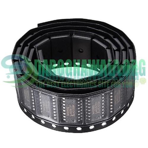 74LS And 74HC Series IC
SMD 74HC595 74HC595D SOP16 Patch 8 Bit Serial Shift Register in Pakistan
74HC595 8-bit Serial-to-Parallel Shift Register is a high-speed shift register that utilizes advanced silicon-gate CMOS technology. This device possesses the high noise immunity and low power consumption of standard CMOS integrated circuits, as well as the ability to drive 15 LS-TTL loads.
This device contains an 8-bit serial-in, parallel-out shift register that feeds an 8-bit D-type storage register. The storage register has 8 3-STATE outputs. Separate clocks are provided for both the shift register and the storage register.
The shift register has direct-overriding clear, serial input, and serial output (standard) pins for cascading. Both the shift register and storage register use positive-edge triggered clocks. If both clocks are connected together, the shift register state will always be one clock pulse ahead of the storage register.
The 74HC logic family is speed, function, and pin-out compatible with the standard 74LS logic family. All inputs are protected from damage due to static discharge by internal diode clamps to VCC and ground.
SKU: D2013 - 74LS And 74HC Series IC
7448 BCD To 7 Segment Decoder Driver IC 74LS48 SN74LS48N 74HC48 in Pakistan
Quick View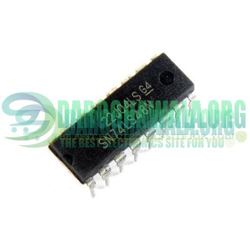 74LS And 74HC Series IC
7448 BCD To 7 Segment Decoder Driver IC 74LS48 SN74LS48N 74HC48 in Pakistan
The 74LS48 features active-high outputs for driving lamp buffers or common-cathode LEDs. They have full ripple-blanking input/output controls and a lamp test input. Display patterns for BCD input count above 9 are unique symbols to authenticate input conditions. Their circuits incorporate automatic leading and/or trailing-edge zero-blanking control (RBI\ and RBO\). Lamp test (LT\) of these types may be performed at any time when the BI\/RBO\ node is at a high level. They contain an overriding blanking input (BI\), which can be used to control the lamp intensity by pulsing or to inhibit the outputs. Inputs and outputs are entirely compatible for use with TTL logic outputs.
SKU: D2010 - 74LS And 74HC Series IC
74151 ic in Pakistan
This Data Selector/Multiplexer contains full on-chip decoding to select one-of-eight data sources as a result of a unique three-bit binary code at the Select inputs. Two complementary outputs provide both inverting and non-inverting buffer operation. A Strobe input is provided which, when at the high level, disables all data inputs and forces the Y output to the low state and the W output to the high state. The Select input buffers incorporate internal overlap features to ensure that select input changes do not cause invalid output transients. RoboticsBD
SKU: D2022


Reviews
There are no reviews yet