- Raspberry Pi & Accessories
- Raspberry Pi Kits
- Raspberry Pi Board
- Raspberry Pi Case
- Raspberry Pi Came
- Raspberry Pi Accessories

74LS And 74HC Series IC
Compare
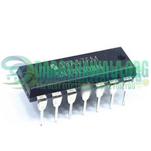
74LS08 74AHS08 SN74LS08N LS08N 7408 QUAD 2-input AND Gate in Pakistan
74LS08 74AHS08 SN74LS08N LS08N 7408 QUAD 2-input AND Gate in Pakistan
₨90
74LS08 74AHS08 SN74LS08N LS08N 7408 QUAD 2-input AND Gate in Pakistan
Features & Specifications
- Four Independent AND Gates
- Standard Pin Configuration
- Fast Switching Times
- Operating Temperature up to 70oC
- High-Speed CMOS Type
- Type: DIP
- Voltage Rating: 2.0 to 6.0V
- Temperature Rating: 0 to 70Deg C
- Number of: 14 Pins
- Mounting: DIP
Package Includes:
- 1 x 74LS08 74AHS08 SN74LS08N LS08N 7408 QUAD 2-input AND Gate in Pakistan
Add a review
You must be logged in to post a review
Log In
Related products
- 74LS And 74HC Series IC
SN74HC163N 74HC163 4-Bit Synchronous Binary Counters IC in Pakistan
Quick View 74LS And 74HC Series IC
SN74HC163N 74HC163 4-Bit Synchronous Binary Counters IC in Pakistan
The SN74HC163 are synchronous, presettable counters that feature an internal carry look-ahead for application in high-speed counting designs. The ’HC163 devices are 4-bit binary counters. Synchronous operation is provided by having all flip-flops clocked simultaneously so that the outputs change coincident with each other when instructed by the count-enable (ENP, ENT) inputs and internal gating. This mode of operation eliminates the output counting spikes normally associated with synchronous (ripple-clock) counters. A buffered clock (CLK) input triggers the four flip-flops on the rising (positive-going) edge of the clock waveform.
These counters are fully programmable; that is, they can be preset to any number between 0 and 9 or 15. As presetting is synchronous, setting up a low level at the load input disables the counter and causes the outputs to agree with the setup data after the next clock pulse, regardless of the levels of the enable inputs.
The clear function for the ’HC163 devices is synchronous. A low level at the clear (CLR\) input sets all four of the flip-flop outputs low after the next low-to-high transition of CLK, regardless of the levels of the enable inputs. This synchronous clear allows the count length to be modified easily by decoding the Q outputs for the maximum count desired. The active-low output of the gate used for decoding is connected to CLR\ to synchronously clear the counter to 0000 (LLLL).
The carry look-ahead circuitry provides for cascading counters for n-bit synchronous applications without additional gating. ENP, ENT, and a ripple-carry output (RCO) are instrumental in accomplishing this function. Both ENP and ENT must be high to count, and ENT is fed forward to enable RCO. Enabling RCO produces a high-level pulse while the count is maximum (9 or 15 with QA high). This high-level overflow ripple-carry pulse can be used to enable successive cascaded stages. Transitions at ENP or ENT are allowed, regardless of the level of CLK.
These counters feature a fully independent clock circuit. Changes at control inputs (ENP, ENT, or LOAD\) that modify the operating mode have no effect on the contents of the counter until clocking occurs. The function of the counter (whether enabled, disabled, loading, or counting) is dictated solely by the conditions meeting the stable setup and hold times.
SKU: D2023 - 74LS And 74HC Series IC
74HC165 Parallel To Serial 8 Bit Shift Register IC in Pakistan
The 74HC165 is a high-speed Si-gate CMOS device and is pin-compatible with low-power Schottky TTL (LSTTL). They are specified in compliance with JEDEC standard no. 7A. The 74HC165 are 8-bit parallel-load or serial-in shift registers with complementary serial outputs (Q7 and Q7) available from the last stage. When the parallel load (PL) input is LOW, parallel data from the D0 to D7 inputs are loaded into the register asynchronously. When PL is HIGH, data enters the register serially at the Ds input and shifts one place to the right (Q0 –> Q1 –> Q2, etc.) with each positive-going clock transition. This feature allows parallel-to-serial converter expansion by tying the Q7 output to the DS input of the succeeding stage. The clock input is a gated-OR structure that allows one input to be used as an active LOW clock enable (CE) input. The pin assignment for the CP and CE inputs is arbitrary and can be reversed for layout convenience. The LOW-to-HIGH transition of input CE should only take place while CP is HIGH for predictable operation. Either the CP or the CE should be HIGH before the LOW-to-HIGH transition of PL to prevent shifting the data when PL is activated.
SKU: D2016 - 74LS And 74HC Series IC
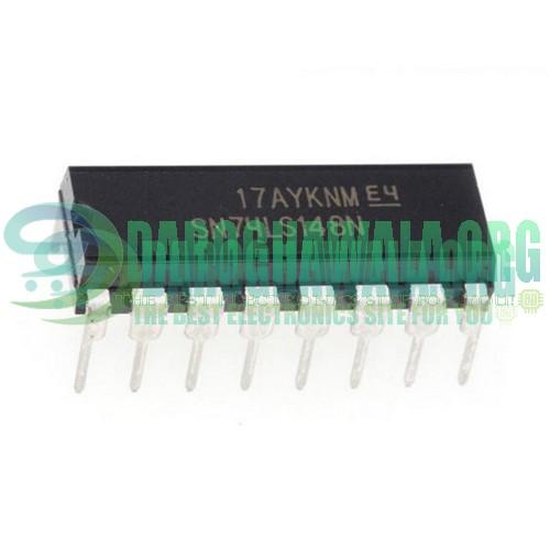
74LS148 3-Bit Priority Encoder IC (74148 IC) DIP-16 in Pakistan
74LS Series ICs are High-Speed Logic gates, ideally a little faster than the 74HC series but more power consumption is required. They are implemented with a Low-Power Schottky diode technology to achieve high switching speed. 74LS148 is one of the 74LS series IC. 74LS148 ICs contain an 8 to 3-Bit priority encoder that converts 8 Data Lines to 3-Line binary. Cascading circuitry (enable input EI and enable output EO) has been provided to allow octal expansion without the need for external circuitry.
SKU: D2024 - 74LS And 74HC Series IC
IC 74LS85 4 Bit Magnitude Comparator DIP 16 in Pakistan
74HC85 4-Bit Comparator IC (7485 IC) DIP-16 Package. 74LS85 is the four-bit magnitude comparators that perform a comparison of straight binary and straight BCD (8-4-2-1) codes. Three fully decoded decisions about two 4-bit words (A, B) are made and are externally available at three outputs. These devices are fully expandable to any number of bits without external gates.
SKU: D2017 - 74LS And 74HC Series IC
7448 BCD To 7 Segment Decoder Driver IC 74LS48 SN74LS48N 74HC48 in Pakistan
Quick View74LS And 74HC Series IC7448 BCD To 7 Segment Decoder Driver IC 74LS48 SN74LS48N 74HC48 in Pakistan
The 74LS48 features active-high outputs for driving lamp buffers or common-cathode LEDs. They have full ripple-blanking input/output controls and a lamp test input. Display patterns for BCD input count above 9 are unique symbols to authenticate input conditions. Their circuits incorporate automatic leading and/or trailing-edge zero-blanking control (RBI\ and RBO\). Lamp test (LT\) of these types may be performed at any time when the BI\/RBO\ node is at a high level. They contain an overriding blanking input (BI\), which can be used to control the lamp intensity by pulsing or to inhibit the outputs. Inputs and outputs are entirely compatible for use with TTL logic outputs.
SKU: D2010


Reviews
There are no reviews yet