- Raspberry Pi & Accessories
- Raspberry Pi Kits
- Raspberry Pi Board
- Raspberry Pi Case
- Raspberry Pi Came
- Raspberry Pi Accessories

74LS And 74HC Series IC
Compare
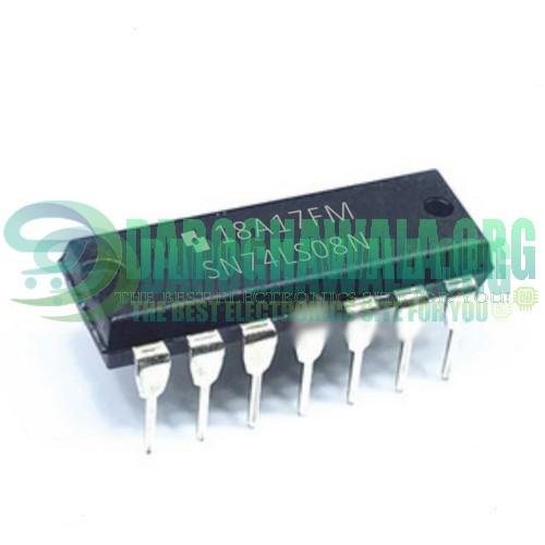
74LS08 74AHS08 SN74LS08N LS08N 7408 QUAD 2-input AND Gate in Pakistan
74LS08 74AHS08 SN74LS08N LS08N 7408 QUAD 2-input AND Gate in Pakistan
₨90
74LS08 74AHS08 SN74LS08N LS08N 7408 QUAD 2-input AND Gate in Pakistan
Features & Specifications
- Four Independent AND Gates
- Standard Pin Configuration
- Fast Switching Times
- Operating Temperature up to 70oC
- High-Speed CMOS Type
- Type: DIP
- Voltage Rating: 2.0 to 6.0V
- Temperature Rating: 0 to 70Deg C
- Number of: 14 Pins
- Mounting: DIP
Package Includes:
- 1 x 74LS08 74AHS08 SN74LS08N LS08N 7408 QUAD 2-input AND Gate in Pakistan
Add a review
You must be logged in to post a review
Log In
Related products
- 74LS And 74HC Series IC
74LS32 74-LS32 74HC32 7432 Quad 2 Input OR Gate DIP IC SN74CH32N in Pakistan
Quick View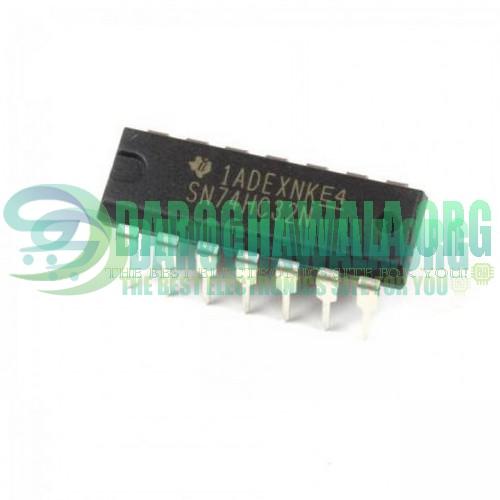 74LS And 74HC Series IC
74LS32 74-LS32 74HC32 7432 Quad 2 Input OR Gate DIP IC SN74CH32N in Pakistan
This device contains four independent gates each of which performs the logic OR function. The 74LS32 is a 14-Pin Quad 2-Input OR Gate IC. The 74LS32 provides four independent 2-input OR gates with standard push-pull outputs. Featured by Sharvi Electronics The device is designed for operation with a power supply range of 2.0V to 6.0V. Inputs include clamp diodes. This enables the use of current-limiting resistors to interface inputs to voltages in excess of VCC.
SKU: D2000 - 74LS And 74HC Series IC
74238 SN74HC238N 74HC238 74LS238 DIP 16 Pin IC in Pakistan
These are high-speed silicon-gate CMOS decoders well suited to memory address decoding or data-routing applications. Both circuits feature low power consumption usually associated with CMOS circuitry, yet have speeds comparable to low-power Schottky TTL logic. Both circuits have three binary select inputs (A0, A1, and A2). If the device is enabled, these inputs determine which one of the eight normally high outputs of the HC/HCT138 series goes low or which of the normally low outputs of the HC/HCT238 series go high. Two active low and one active high enables (E1, E2, and E3)are provided to ease the cascading of decoders. The decoder’s eight outputs can drive ten low-power Schottky TTL equivalent loads.
SKU: D2021 - 74LS And 74HC Series IC
74HC157 Quad 2×1 Multiplexer MUX DIP IC SN74LS157N 74157 74-LS157 in Pakistan
Quick View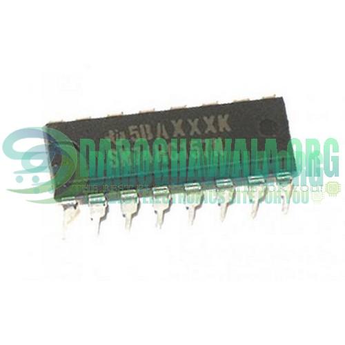 74LS And 74HC Series IC
74HC157 Quad 2×1 Multiplexer MUX DIP IC SN74LS157N 74157 74-LS157 in Pakistan
74HC157 is a high-speed multiplexer integrated circuit consisting of four 2-input digital multiplexers inside the chip. It is pin-compatible with Low-power Schottky TTL. It has two control inputs namely enable and select input. Additionally, it has two groups of registers. The selected input determines the register from which the data comes. Its operation is specified over a temperature range of -55 °C to 125 °C.
SKU: D2001 - 74LS And 74HC Series IC
74LS138 – 3 to 8 Decoder De-Multiplexer IC in Pakistan
The 74LS138 is a 3:8 Decoder IC that is commonly used in decoding or de-multiplexing circuits for memory decoding or data routing purposes. It is designed for high-speed operations and has three enable pins to make it easier to cascade with other ICs. The device decodes 1-of-8 lines, set by x3 binary select inputs & three enable inputs. The LS138 can be used as an 8- output demultiplexer by using one active LOW Enable input as data input & the other Enable inputs as strobes. The IC has an operating voltage from 1.0V to 5.5V with a low power consumption of 32mW. The propagation delay is around 21nS.
SKU: D2020 - 74LS And 74HC Series IC
74HC165 Parallel To Serial 8 Bit Shift Register IC in Pakistan
The 74HC165 is a high-speed Si-gate CMOS device and is pin-compatible with low-power Schottky TTL (LSTTL). They are specified in compliance with JEDEC standard no. 7A. The 74HC165 are 8-bit parallel-load or serial-in shift registers with complementary serial outputs (Q7 and Q7) available from the last stage. When the parallel load (PL) input is LOW, parallel data from the D0 to D7 inputs are loaded into the register asynchronously. When PL is HIGH, data enters the register serially at the Ds input and shifts one place to the right (Q0 –> Q1 –> Q2, etc.) with each positive-going clock transition. This feature allows parallel-to-serial converter expansion by tying the Q7 output to the DS input of the succeeding stage. The clock input is a gated-OR structure that allows one input to be used as an active LOW clock enable (CE) input. The pin assignment for the CP and CE inputs is arbitrary and can be reversed for layout convenience. The LOW-to-HIGH transition of input CE should only take place while CP is HIGH for predictable operation. Either the CP or the CE should be HIGH before the LOW-to-HIGH transition of PL to prevent shifting the data when PL is activated.
SKU: D2016


Reviews
There are no reviews yet