- Raspberry Pi & Accessories
- Raspberry Pi Kits
- Raspberry Pi Board
- Raspberry Pi Case
- Raspberry Pi Came
- Raspberry Pi Accessories

74LS And 74HC Series IC
Compare
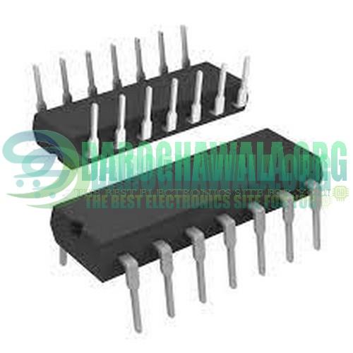
7437 Quad Two input NAND in Pakistan
7437 Quad Two input NAND in Pakistan
₨87
7437 Quad Two input NAND in Pakistan
Packing list:
- 1x 7437 Quad Two input NAND
Add a review
You must be logged in to post a review
Log In
Related products
- 74LS And 74HC Series IC
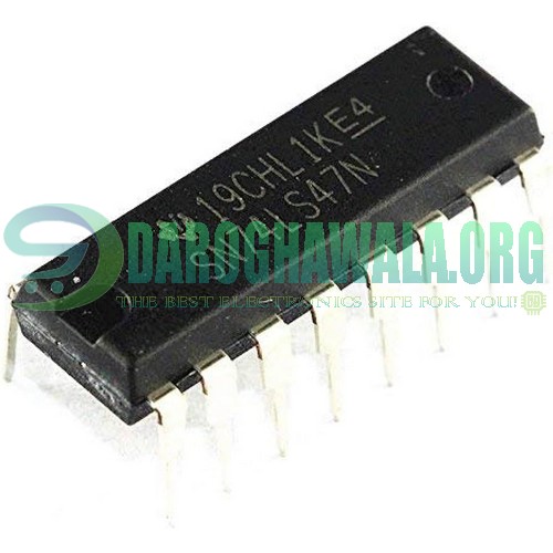
7447 74HC47 74LS47 BCD to 7 Segment Decoder Driver DIP 16 in Pakistan
Quick View 74LS And 74HC Series IC
7447 74HC47 74LS47 BCD to 7 Segment Decoder Driver DIP 16 in Pakistan
74LS47 accepts four lines of BCD (8421) input data, generates their complements internally and decodes the data with seven AND/OR gates having open-collector outputs to drive indicator segments directly. Each segment output is guaranteed to sink 24 mA in the ON (LOW) state and withstand 15V in the OFF (HIGH) state with a maximum leakage current of 250 µA. Auxiliary inputs provided blanking, 74LS47 BCD to 7-Segment Decoder/Driver IC.
SKU: D2008 - 74LS And 74HC Series IC
SN74HC163N 74HC163 4-Bit Synchronous Binary Counters IC in Pakistan
Quick View74LS And 74HC Series ICSN74HC163N 74HC163 4-Bit Synchronous Binary Counters IC in Pakistan
The SN74HC163 are synchronous, presettable counters that feature an internal carry look-ahead for application in high-speed counting designs. The ’HC163 devices are 4-bit binary counters. Synchronous operation is provided by having all flip-flops clocked simultaneously so that the outputs change coincident with each other when instructed by the count-enable (ENP, ENT) inputs and internal gating. This mode of operation eliminates the output counting spikes normally associated with synchronous (ripple-clock) counters. A buffered clock (CLK) input triggers the four flip-flops on the rising (positive-going) edge of the clock waveform.
These counters are fully programmable; that is, they can be preset to any number between 0 and 9 or 15. As presetting is synchronous, setting up a low level at the load input disables the counter and causes the outputs to agree with the setup data after the next clock pulse, regardless of the levels of the enable inputs.
The clear function for the ’HC163 devices is synchronous. A low level at the clear (CLR\) input sets all four of the flip-flop outputs low after the next low-to-high transition of CLK, regardless of the levels of the enable inputs. This synchronous clear allows the count length to be modified easily by decoding the Q outputs for the maximum count desired. The active-low output of the gate used for decoding is connected to CLR\ to synchronously clear the counter to 0000 (LLLL).
The carry look-ahead circuitry provides for cascading counters for n-bit synchronous applications without additional gating. ENP, ENT, and a ripple-carry output (RCO) are instrumental in accomplishing this function. Both ENP and ENT must be high to count, and ENT is fed forward to enable RCO. Enabling RCO produces a high-level pulse while the count is maximum (9 or 15 with QA high). This high-level overflow ripple-carry pulse can be used to enable successive cascaded stages. Transitions at ENP or ENT are allowed, regardless of the level of CLK.
These counters feature a fully independent clock circuit. Changes at control inputs (ENP, ENT, or LOAD\) that modify the operating mode have no effect on the contents of the counter until clocking occurs. The function of the counter (whether enabled, disabled, loading, or counting) is dictated solely by the conditions meeting the stable setup and hold times.
SKU: D2023 - 74LS And 74HC Series IC
74LS138 – 3 to 8 Decoder De-Multiplexer IC in Pakistan
The 74LS138 is a 3:8 Decoder IC that is commonly used in decoding or de-multiplexing circuits for memory decoding or data routing purposes. It is designed for high-speed operations and has three enable pins to make it easier to cascade with other ICs. The device decodes 1-of-8 lines, set by x3 binary select inputs & three enable inputs. The LS138 can be used as an 8- output demultiplexer by using one active LOW Enable input as data input & the other Enable inputs as strobes. The IC has an operating voltage from 1.0V to 5.5V with a low power consumption of 32mW. The propagation delay is around 21nS.
SKU: D2020


Reviews
There are no reviews yet