- Raspberry Pi & Accessories
- Raspberry Pi Kits
- Raspberry Pi Board
- Raspberry Pi Case
- Raspberry Pi Came
- Raspberry Pi Accessories
74LS And 74HC Series IC
Compare
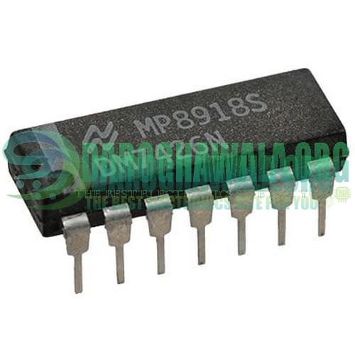
7426 Quad Two input NAND, High voltage in Pakistan
7426 Quad Two input NAND, High voltage in Pakistan
₨57
7426 Quad Two input NAND, High voltage in Pakistan
Packing list:
- 1x 7426 Quad Two input NAND, High voltage
Add a review
You must be logged in to post a review
Log In
Related products
- 74LS And 74HC Series IC
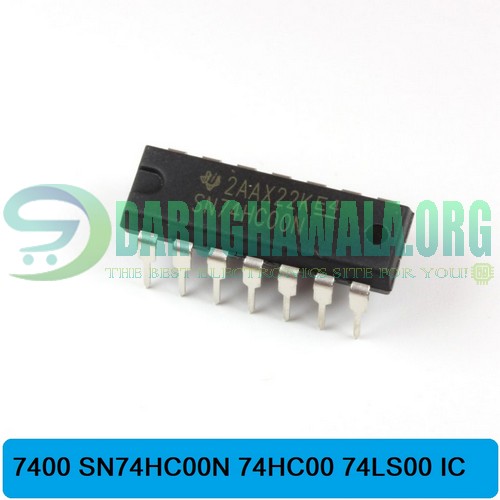
74LS32 74-LS32 74HC32 7432 Quad 2 Input OR Gate DIP IC SN74CH32N in Pakistan
Quick View 74LS And 74HC Series IC
74LS32 74-LS32 74HC32 7432 Quad 2 Input OR Gate DIP IC SN74CH32N in Pakistan
This device contains four independent gates each of which performs the logic OR function. The 74LS32 is a 14-Pin Quad 2-Input OR Gate IC. The 74LS32 provides four independent 2-input OR gates with standard push-pull outputs. Featured by Sharvi Electronics The device is designed for operation with a power supply range of 2.0V to 6.0V. Inputs include clamp diodes. This enables the use of current-limiting resistors to interface inputs to voltages in excess of VCC.
SKU: D2000 - 74LS And 74HC Series IC
74238 SN74HC238N 74HC238 74LS238 DIP 16 Pin IC in Pakistan
These are high-speed silicon-gate CMOS decoders well suited to memory address decoding or data-routing applications. Both circuits feature low power consumption usually associated with CMOS circuitry, yet have speeds comparable to low-power Schottky TTL logic. Both circuits have three binary select inputs (A0, A1, and A2). If the device is enabled, these inputs determine which one of the eight normally high outputs of the HC/HCT138 series goes low or which of the normally low outputs of the HC/HCT238 series go high. Two active low and one active high enables (E1, E2, and E3)are provided to ease the cascading of decoders. The decoder’s eight outputs can drive ten low-power Schottky TTL equivalent loads.
SKU: D2021 - 74LS And 74HC Series IC
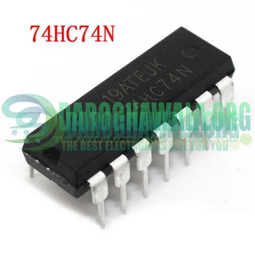
74LS76 DUAL JK FLIP-FLOP IC in Pakistan
74LS76 comes with dual JK flip-flops. JK flip flops are widely used in daily electronics devices by many methods but the basic operation of the JK flip flop is to store a bit. JK flip flop allows it to store a bit and then allows it to use for further functions. in digital electronics circuits. JK flip flop is one of the popular flip flops due to its clock input, pre-set, and clear functionalities. The JK flip-flop changes its state under the clock pulse signal. The clock signal can be either a positive edge or a negative edge. The clock pulse gives multiple advantages to the flip-flop. 74LS76 also has provided a feature to neglect or prevent invalid outputs.
SKU: D2025


Reviews
There are no reviews yet